E-mail: cysi@cysi.wang


ICP (Inductively Coupled Plasma) plasma etching technology is an etching process that generates high-density plasma by inductive coupling.

ICP (Inductively Coupled Plasma) plasma etching technology is an etching process that generates high-density plasma by inductive coupling. ICP plasma etcher usually uses a high-frequency power supply to excite the gas to generate high-density plasma, which is different from traditional DC or RF plasma systems.
High-density plasma: ICP technology can generate high-density plasma, which makes the etching rate high, and operates at a lower pressure, which can improve the accuracy and consistency of etching.
Highly selective etching: The etching depth and speed can be precisely controlled, which is suitable for complex semiconductor materials and thin film etching.
Good etching uniformity: ICP plasma etcher can provide a relatively uniform etching effect, which is suitable for large-scale production occasions with high process accuracy requirements.
Low-damage processing: Since the energy of the plasma is relatively uniform and controllable, the damage to the material during the etching process is small, which is especially suitable for high-precision and thin film processing.
Widely used: ICP etcher is widely used in semiconductor manufacturing, microelectronic device processing, MEMS (micro-electromechanical system), solar cells, LED, photolithography film and nanotechnology.
Plasma generation: The inductor coil is excited by a high-frequency power supply to generate a high-density plasma. Gas (such as fluorinated gas, oxygen, argon, etc.) is usually used as the working gas.
Ion acceleration: Under the action of the electric field, the ions in the plasma are accelerated and react with the sample surface for etching.
Etching reaction: The ions and free radicals in the working gas react chemically with the sample surface to remove unwanted materials, thereby achieving fine etching.
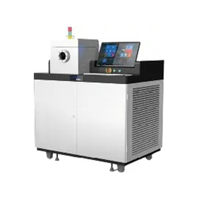
Reaction chamber: used to accommodate samples and plasma, usually made of corrosion-resistant materials such as stainless steel.
RF source: Generates radio frequency signals to excite the inductor coil and generate plasma.
Gas delivery system: used to introduce reactive gas into the reaction chamber.
Vacuum system: Controls the pressure in the chamber to keep it within the appropriate etching range.
Sample stage: used to support the material or chip to be etched, and can be temperature controlled and adjusted.
Vacuum chamber size | Ф 300mm (or Ф 350mm) × H300mm |
Number and size of samples | Ф 6-inch (or 8-inch) 1 piece, or multiple pieces in bulk |
Etching non-uniformity | ±3% - ±5% |
Vacuum index | Ultimate vacuum: ≤2×10^−4Pa |
Evacuation rate | The system is filled with dry N_2 to release the vacuum, and then evacuated to 9× 10^−4 Pa≤40min after short exposure to the atmosphere |
Etching gas | Fluorine-based or weaker corrosive gases |
Etching rate | 0.5-4μm/min (depending on the specific material and process) |
Workbench | Automatic lifting and lowering, the etching distance can be adjusted within the range of 60mm-120mm. Including independent water cooling, controlling the sample stage temperature at 10℃ - 35℃ |
Power supply configuration | Upper electrode (coupling electrode): 1000W, RF power supply, including automatic matching Lower electrode (bias electrode): 600W, RF power supply, including automatic matching |
Operation mode | Fully automatic + semi-automatic control |
Plasma Etcher (ICP, Inductively Coupled Plasma Etching) Application Cases
Background ICP (inductively coupled plasma) etching technology is an important processing technology in modern semiconductor manufacturing, microelectronics processing, optoelectronic devices and MEMS (microelectromechanical systems) and other fields. Its working principle is to generate high-density plasma for physical and chemical etching, and is widely used in high-precision and high-selectivity etching processes.
The following is a typical application case of ICP plasma etcher, which introduces how to use this technology for micro-processing in semiconductor manufacturing.
Application Case: ICP plasma etching in semiconductor chip manufacturing
Background
In the manufacturing process of semiconductor chips, the post-lithography etching process is one of the most important steps, which is mainly used to transfer the lithography pattern to the thin film layer of the chip. Especially for semiconductor devices with multi-layer structures, the etching process must have high selectivity and fine control to ensure that the patterns between different material layers are clear, accurate and damage-free.
Application steps
Step 1: Material preparation
1. Select the material to be etched:
1. In semiconductor manufacturing, common materials to be etched include metals or dielectric materials such as silicon (Si), silicon nitride (Si₃N₄), silicon oxide (SiO₂), tantalum (Ta), and aluminum (Al).
2. These materials are usually subjected to photolithography to form the required micropatterns.
2. Apply photoresist:
1. Use spin coating to evenly apply photoresist on the surface of the material.
2. Then perform UV exposure, use a photomask to transfer the pattern to the photoresist, and form a mask layer after development.
Step 2: Load the sample and set the etching process
1. Place the sample in the ICP etcher:
Place the photolithographically processed silicon wafer (or other material sheet) in the fixture of the ICP plasma etcher to ensure that the sample is firmly fixed.
2. Select appropriate gas and working parameters:
ICP etcher generates high-density plasma through plasma excitation, so it is necessary to select appropriate gas (such as fluorinated gas CF₄, SF₆, chlorinated gas Cl₂ or oxygen O₂, etc.) and mixed gas to achieve the desired etching effect.
Set power: The working principle of the ICP system is to generate plasma through inductively coupled electric fields, so the power supply power needs to be set. High-frequency (13.56 MHz or other frequencies) power supply can produce high-density plasma.
Control gas pressure: Gas pressure control is an important parameter in ICP etching, usually in the range of a few mTorr to tens of mTorr.
Set gas flow rate: Select appropriate gas flow rate to ensure the stability and efficiency of etching.
3. Etching time and depth control:
According to the pattern size and depth requirements of the etching, set the appropriate etching time. By accurately controlling the time, the desired etching depth can be achieved.
Step 3: Perform ICP etching
1. Start plasma etching:
Start the ICP etcher to excite high-density plasma. The ions, electrons, and free radicals in the plasma react with the material to be etched, removing the material from the surface.
The etching process may involve both physical etching (ion impact) and chemical etching (reaction to generate volatile compounds), and the dominant role may be different depending on the type of gas.
2. Monitor the progress of etching:
The progress of etching is monitored in real time by the monitoring system in the etcher. Optical monitoring, reflectivity monitoring, and other techniques can be used to ensure the accuracy of etching and the quality of pattern transfer.
Step 4: Post-processing and cleaning
Remove the photoresist:
After etching, use a solvent (such as acetone or isopropyl alcohol) or plasma cleaning to remove the residual photoresist.
After cleaning, rinse the sample thoroughly with deionized water to remove any solvent or chemical residues.
Drying:
Dry the sample with nitrogen or air to ensure that there is no moisture remaining.
Step 5: Inspection and verification
1. Inspection using a scanning electron microscope (SEM):
Use SEM to observe the microstructure after etching to ensure that the pattern is clear, the size is accurate, and there is no over-etching or nicking.
2. Verify the etching depth:
Use a profilometer or other depth measuring instrument to check whether the etching depth meets the requirements.
Step 6: Further manufacturing process
After the etching process is completed, other processes such as metal deposition, oxidation, diffusion, etc. may be carried out to complete the manufacturing of semiconductor chips.
Case summary
In the semiconductor chip manufacturing process, ICP etcher can achieve high-precision and high-selectivity etching due to its high-density plasma characteristics. By precisely controlling parameters such as gas composition, power, gas pressure and etching time, ICP etcher can be applied to complex micro-machining needs, such as selective etching of multi-layer materials, micro-structure processing of metal or dielectric layers, etc.
The application of this etching technology greatly improves the accuracy and efficiency of chips, while reducing the risk of device damage, enabling chip manufacturers to produce more complex and high-performance semiconductor devices.
If you are interested in our plasma etcher ICP, please contact us for more information and quotes.
Tel: 185 3800 8121
Email: Lily@cysitech.com
Contact: Zhao Xiaoli
WeChat: 15617818691


Copyright © Zhengzhou CY Scientific Instrument Co., Ltd. All Rights Reserved Update cookies preferences
| Sitemap | Technical Support: 


