E-mail: cysi@cysi.wang


In plasma etcher, CCP (Capacitively Coupled Plasma) is a common plasma etching technology, and its principles and characteristics are as follows

In plasma etcher, CCP (Capacitively Coupled Plasma) is a common plasma etching technology, and its principles and characteristics are as follows:
CCP plasma is generated by driving electrodes with radio frequency (RF) power supply. Usually includes the following parts:
Upper and lower electrode structure:
The lower electrode is connected to the RF power supply (usually at a frequency of 13.56 MHz).
The upper electrode can be grounded or achieve specific functions through a matching network.
Gas environment: Etching gas is introduced into the reaction chamber, and plasma is formed by electric field excitation. Ions and active neutral particles in the plasma complete etching.
When working, the RF power supply drives the lower electrode to generate a strong electric field, which ionizes the gas to form plasma and forms a sheath layer at the same time, so that the ions bombard the substrate surface vertically to complete etching.
Strong etching directionality:
The electric field is mainly perpendicular to the substrate, which is suitable for anisotropic etching.
Etching uniformity:
By optimizing the electrode spacing and gas flow distribution, better etching uniformity can be achieved.
Scope of application:
Applicable to most materials (such as silicon, oxides, nitrides, etc.) and fine pattern etching.
Energy regulation:
RF power and gas ratio can adjust the etching rate and selectivity.
Semiconductor manufacturing (such as photoresist removal, silicon etching).
Microelectromechanical system (MEMS) processing.
Flat panel display manufacturing (TFT-LCD etching).
Optical device processing.
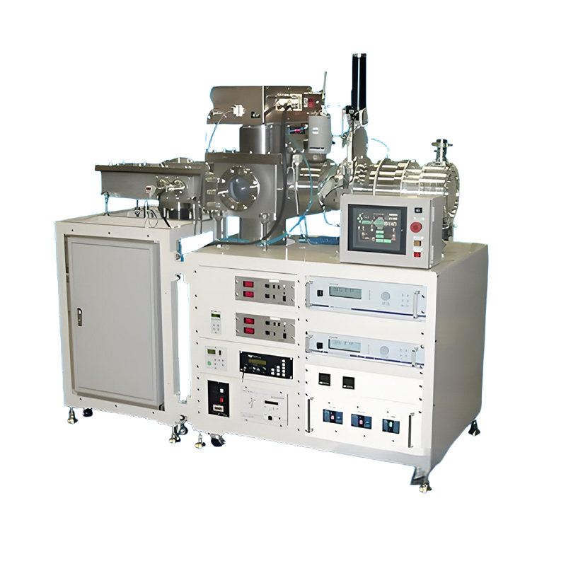
If you are interested in our plasma etcher CCP, please contact us for more information and quotation.
Tel: 185 3800 8121
Email: Lily@cysitech.com
Contact person: Zhao Xiaoli
WeChat: 15617818691
The relevant parameters of CCP (capacitively coupled plasma) system are usually closely related to the performance of the equipment, processing requirements and etching process. The following is the classification of important parameters of CCP system and their typical range and impact:
RF parameters
| RF frequency | Common frequencies: 13.56 MHz (mainstream industrial standard), as well as low frequencies (such as 400 kHz) and dual-frequency systems (such as 13.56 MHz + 2 MHz). Frequency determines the coupling efficiency of the electric field, which in turn affects the ion density and etching rate. |
RF power | Range: 50 W to several thousand W, depending on the process and equipment scale. Impact: The higher the power, the greater the ion density and the faster the etching rate; but too high power may cause over-etching or damage the substrate. | |
Reaction chamber parameters
| Electrode spacing | Range: 1 to 5 cm. Impact: Smaller spacing enhances the electric field strength and is conducive to the generation of high-density plasma; larger spacing is conducive to etching uniformity. |
Electrode size | Range: Determined by wafer size (typical values are 200 mm, 300 mm, or larger). Impact: The size of the electrode directly affects the coverage of the plasma and the uniformity of etching. | |
Process gas parameters
| Gas type | Commonly used gases: CF₄, SF₆, O₂, Cl₂, Ar, H₂, etc., selected according to the etching material. Impact: Gas chemistry determines etching selectivity, etching rate, and post-etching surface quality. |
Gas flow rate | Range: 10 to 500 sccm, depending on chamber size and process requirements. Impact: Flow rate affects plasma density and chemical reaction rate. | |
Vacuum parameters
| Working pressure | Range: 10⁻¹ to tens of Pa (typical values are 1 to 10 Pa). Impact: Lower pressure enhances ion energy and facilitates anisotropic etching; higher pressure enhances chemical reactivity and facilitates selective etching. |
Vacuum base pressure | Range: 10⁻⁵ to 10⁻⁶ mbar (initial vacuum before reaction). Impact: Lower base pressure ensures the purity of the reaction chamber and reduces the impact of impurity gases. | |
Etching performance parameters
| Etching rate | Range: tens to hundreds of nm/min (depending on the material and process). Impact: Etching rate needs to match the pattern size, etching depth and process time. |
Etching uniformity | Standard: ±1 to 5%. Impact: Uniformity is affected by gas flow distribution, electrode design and electric field distribution. | |
Etching selectivity | Common range: 10:1 to 50:1 (target material to mask material). Impact: High selectivity reduces mask material consumption and ensures pattern accuracy. | |
Plasma parameters
| Ion density | Range: 10⁹ ~ 10¹² cm⁻³. Impact: The higher the density, the faster the etching rate, but it also increases the risk of substrate damage. |
Electron temperature | Range: 1 ~ 5 eV. Impact: The electron temperature affects the chemical reaction rate and ion bombardment energy. | |
Temperature control parameters
| Electrode temperature | Range: -10°C ~ 100°C (or higher). Impact: Low temperature helps mask protection, and high temperature accelerates chemical reactions. |
Substrate temperature | Range: -50°C ~ 300°C (or higher). Impact: The substrate temperature directly affects the fineness and surface quality of the etched pattern. | |
Monitoring and feedback parameters | RF bias | Typical range: tens to hundreds of V (DC bias). Impact: The bias determines the energy of ion bombardment of the substrate and affects the etching directionality. |
Optical emission spectroscopy (OES) | Used to monitor active particles in the etching atmosphere in real time. | |
End point detection | Method: Spectral monitoring, quality monitoring, etc., used to determine the end of the etching process |
Plasma Etcher (CCP, Capacitive Coupled Plasma Etching) Application Cases
Background CCP (capacitive coupled plasma) etching technology has important applications in semiconductor manufacturing, microelectronics processing, thin film material processing and other fields. The CCP system transfers high-frequency electrical energy to the plasma through capacitive coupling, generating high-energy ion beams in a low-pressure environment for micro-etching, surface cleaning, thin film deposition and other operations. Unlike ICP (inductively coupled plasma) etching, the CCP power supply excites the plasma through capacitive coupling between the electrode and the plasma, and is generally suitable for low to medium energy etching processes.
The following is a typical application case of the CCP plasma etcher, describing how to apply this technology for micro-machining in semiconductor chip manufacturing.
Application Case: CCP plasma etching in semiconductor chip manufacturing
Background
In the semiconductor manufacturing process, different layers of materials on the chip (such as silicon, metal, oxide, etc.) need to be accurately transferred through the etching process to transfer the photolithography pattern. CCP etching technology is generally used for high-precision etching of dielectric layers, metal layers or thin films due to its adjustable plasma characteristics, especially when high selectivity and low damage are required.
Application steps
Step 1: Material preparation
Select the material to be etched:
Common etching materials include: silicon (Si), silicon oxide (SiO₂), silicon nitride (Si₃N₄), aluminum (Al), titanium (Ti), etc. These materials are usually used at different levels in semiconductor manufacturing.
Coating photoresist:
Use spin coating to apply photoresist, and perform exposure and development to form the required pattern. This process is very important because the etched pattern needs to be accurately transferred to the material to be processed.
Step 2: Load the sample and set the etching process
Put the sample into the CCP etcher:
1.Put the sample coated with photoresist and exposed into the sample holder of the etcher.
2. Make sure the sample surface is clean and flat to avoid uneven etching during the etching process.
Select appropriate gas and working parameters:
1. Depending on the material, select appropriate gas, such as chlorine (Cl₂), fluorinated gas (CF₄), oxygen (O₂), chlorofluorinated gas (SF₆), etc.
2. Adjust parameters such as power, gas flow, pressure, etc. CCP etcher usually excites plasma through power supply, generates electric field through capacitive coupling, and thus excites plasma.
Set gas flow and working pressure:
Typical CCP etching systems operate in a low-pressure environment (about 5-100 mTorr), and control the rate and quality of etching by adjusting gas flow rate and system pressure.
Select etching time and power setting:
1. The setting of etching time is very critical. Too long etching time will lead to over-etching, while too short etching time may not be able to transfer the pattern completely.
2. Appropriate power setting ensures the formation of stable plasma and ensures the uniformity of etching effect.
Step 3: Perform CCP etching
Start plasma etching:
1. Start the CCP etcher, and the power supply excites plasma through the principle of capacitive coupling to form high-energy ions and neutral particles.
2. Under the action of the electric field, the plasma reacts with the material to be etched, thereby removing the unwanted material on the surface.
Etching process control:
1. During the etching process, it is necessary to monitor the stability of the plasma and the etching state of the sample in real time. The etching depth can be precisely controlled by adjusting parameters such as gas flow, power, and pressure.
2. The main method of etching is a combination of chemical reaction and physical collision. The specific reaction type depends on the gas used.
Step 4: Post-processing and cleaning
Removing photoresist:
After etching, the residue of the photoresist needs to be removed. The common method is to use a solvent (such as acetone or isopropanol) to remove it, or use plasma treatment to remove the glue layer.
Cleaning samples:
Use deionized water to clean the sample to remove any solvent or chemical residue to ensure the cleanliness of the sample.
Drying:
Use nitrogen or air to blow dry the sample to prevent contamination or corrosion caused by residual moisture.
Step 5: Inspection and verification
1. Use a scanning electron microscope (SEM) to check the etched pattern:
Use SEM to check the etched pattern to ensure the etching accuracy and pattern integrity. Check for over-etching or under-etching.
2. Perform etching depth test:
Use a profilometer or other precision measuring tools to check the etching depth to ensure that it meets the design requirements.
Step 6: Further manufacturing process
After etching, it may be necessary to continue other processes such as thin film deposition, diffusion, metallization, etc. to complete the manufacture of semiconductor chips or other electronic devices.
Case summary
In the semiconductor manufacturing process, CCP plasma etcher is widely used in various micro-machining processes, especially in etching processes that require high selectivity and fine control. By precisely adjusting parameters such as gas composition, pressure, power and etching time, CCP etching technology can meet the etching requirements of multi-layer materials and maintain low surface damage. It is suitable for etching silicon wafers, metal films, oxide layers, etc.
For example, in semiconductor transistor manufacturing, CCP etching is used to etch metal layers (such as aluminum) or dielectric layers (such as silicon dioxide) to form microstructures to ensure the function and performance of the chip. At the same time, this technology is also used in fields with high precision requirements such as etching optoelectronic components, MEMS devices, and some thin film optical devices.


Copyright © Zhengzhou CY Scientific Instrument Co., Ltd. All Rights Reserved Update cookies preferences
| Sitemap | Technical Support: 


