E-mail: cysi@cysi.wang


Ion beam etching (IBE) is a physical vapor etching technology widely used in semiconductor, optoelectronics, nanotechnology and other fields.

Ion beam etching (IBE) is a physical vapor etching technology widely used in semiconductor, optoelectronics, nanotechnology and other fields. Its principle is to accelerate ion beam to bombard the material surface and use the kinetic energy of ions to remove material atoms from the surface, thereby achieving etching processing.
Application
Ion beam etching (IBE) is a kind of high precision etching technology, which is widely used in semiconductor manufacturing, MEMS, nanotechnology and optoelectronics. Its unique physical etching mechanism allows it to provide very fine etching control for a variety of high-precision machining scenarios. Although its etching rate is low, IBE is still a valuable technology choice in applications requiring high accuracy and low damage.
Purchase information
If you are interested in our evaporation coater, please contact us for more information.
Tel:138 3857 9492
Email:carol@cysitech.com
Contact:Carol Xu
Wechat:15290599353
WhatsApp/Skype: 13838579492
Technical parameters
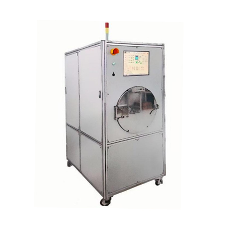
Product name | Ion Beam Etcher | |
Product model | CY-IBE-FA100 | CY-IBE-100S |
Sample size | 4inch and below | |
RF ion source | The ion energy is 100~1000V, the ion flux is 100~800mA, the beam collimation is <±5%, the beam non-uniformity is <±5%, and the process stability time is 100h | |
Molecular pump | 1000/2000/3000(L/s), can be equipped with corrosion type pump | |
Backing pump | Mechanical pump/dry pump, can be equipped with anti-corrosion pump | |
Forepump | Mechanical pump/dry pump, can be equipped with anti-corrosion pump | |
Pre-pumped chamber | Optional | |
Process pressure control | No control pressure /0~1Torr control pressure | |
Gas type | H2/CH4/O2/N2/Ar/SF6/CF4/CHF3/C4F8/NF3/NH3/C2F6/Cl2/BCl3/HBr/ Customized (Up to 12 channels) | |
Gas range | 0~5sccm/50sccm/100sccm/Customized | |
Transfer chamber | Optional | |
Sample temperature control | -30℃/10℃~RT | |
Sample holder | Rotation 0~30rpm, support reciprocating motion, 0~180° tilt, control accuracy ±0.1°, automatic control | |
Control system | Fully automatic/Customized | |
Work mode | Can choose Reactive ion Beam Etching Mode (RIBE) or Chemically Assisted ion Beam Etching Mode (CAIBE) | |
Dimension | L820mm*W1320mm*H1950mm | |
Weight | ~400KGS | |
Case: Ion beam etching in optoelectronic devices
Step 1: Material preparation
Choose appropriate optoelectronic materials:
The materials of optoelectronic devices usually include gallium nitride (GaN), gallium arsenide (GaAs), silicon (Si), silicon photonic materials, optical waveguide materials, etc.
These materials are usually in thin film form and may need to be attached to a substrate (such as a silicon wafer, sapphire substrate, etc.).
Surface cleaning:
Before ion beam etching, make sure that there are no contaminants or oxides on the surface of the material.
Plasma cleaning (such as oxygen plasma) or solvent cleaning is used to remove organic contaminants.
Use ultrasonic cleaning or deionized water cleaning to remove surface particles.
Step 2: Photolithography and patterning
Coating photoresist:
Evenly coat the surface of the material with photoresist (e.g., photosensitive resin).
The photoresist is applied by spin coating to ensure that the thickness of the layer is uniform, usually tens of microns.
Exposure and development:
Use a photolithography machine for ultraviolet (UV) exposure, and project the desired micro pattern onto the photoresist through a mask.
After exposure, the photoresist in the unexposed part is removed by development, leaving a protective layer as an etching mask.
Hardening the photoresist:
The photoresist is hardened by heat baking or light baking to increase its etching resistance.
Step 3: Ion beam etching
Loading the material into the IBE equipment:
The material coated with photoresist is placed in the working chamber of the ion beam etcher.
Make sure the material is properly fixed and set the appropriate tilt angle or rotation to achieve uniform etching.
Select gas and set etching conditions:
Argon (Ar) is usually used as the ion source, and chlorine (Cl₂), fluorinated gas (such as SF₆) or oxygen (O₂) may be added, depending on the properties of the etched material.
Set the voltage of the ion source to control the energy of the ion beam. Usually, the energy range is between tens to hundreds of electron volts (eV) to ensure etching accuracy and selectivity.
Set the appropriate gas pressure and gas flow according to the properties of the target material to control the etching rate.
Perform ion beam etching:
Start the ion beam etching process. The ion beam is accelerated by an electric field and hits the surface of the material, physically removing the material under the photoresist.
During the etching process, the ion beam bombards the material surface in a vertical direction to ensure high-precision etching.
Monitor the etching process:
Use an optical microscope or other surface analysis tools to monitor the etching depth and effect in real time to ensure the transfer of the pattern and the selectivity of the etching.
Optimize the etching effect by adjusting the intensity of the ion beam, etching time and other parameters.
Step 4: Post-processing and cleaning
Remove the photoresist:
After etching, remove the protective layer (photoresist) to reveal the etched microstructure. Solvents (such as acetone) or plasma cleaning are usually used to remove the photoresist.
Post-etch cleaning:
Use deionized water or organic solvents to clean the surface of the etched material to remove possible residual contaminants.
If necessary, nitrogen drying or drying can be performed.
Step 5: Etching quality inspection and optimization
Surface inspection:
Use a scanning electron microscope (SEM) to inspect the etched microstructure to ensure that the size and shape meet the requirements.
Check the etching depth, edge smoothness and material damage.
Performance test:
Perform performance test on the optoelectronic devices after etching to ensure that their functions meet expectations, such as the photoelectric conversion efficiency of laser diodes and the transmission characteristics of optical waveguides.
Summary
Through ion beam etching, the manufacture of optoelectronic devices can ensure precision while avoiding material damage caused by chemical etching methods. The high selectivity and low damage of IBE technology make it very suitable for high-precision etching, especially in the processing of optoelectronic materials and devices. The application cases of ion beam etching demonstrate its unique advantages in the manufacture of microstructures, especially in the fields of nanoscale patterns, micro optical waveguides and integrated optical circuits.


Copyright © Zhengzhou CY Scientific Instrument Co., Ltd. All Rights Reserved Update cookies preferences
| Sitemap | Technical Support: